PCBPath について: 世界的な高速ターン PCB 製造およびターンキー PCBA メーカー
2015 年に設立された PCBPath は、世界的なハードウェア イノベーター向けのラピッド PCB プロトタイピング、高度な HDI 製造、エンドツーエンドのターンキー PCBA アセンブリを専門とする ISO 認定の直接メーカーです。
Accelerating Electronic Innovation with Intelligent Manufacturing
2015 年に設立された PCBPath は、世界的なハードウェア イノベーター向けのラピッド PCB プロトタイピング、高度な HDI 製造、エンドツーエンドのターンキー PCBA アセンブリを専門とする ISO 認定の直接メーカーです。
私たちとは: あらゆる層におけるイノベーション
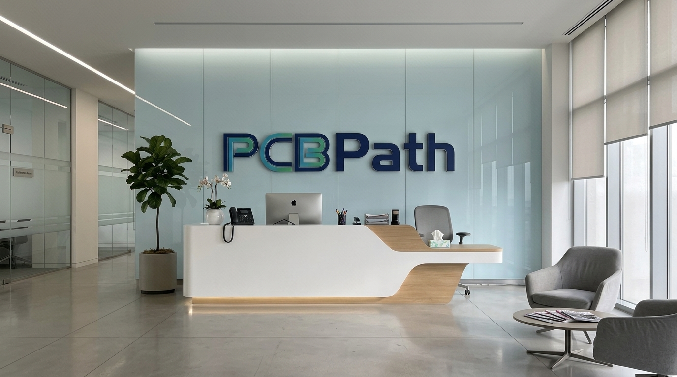
2015年に設立され、 PCBパス は、高精度のプリント基板 (PCB) 製造およびターンキー PCB アセンブリ (PCBA) を専門とする一流の直接メーカーです。当社は、ラピッドエンジニアリングプロトタイプとスケーラブルな量産の間の橋渡しをし、自動車、産業オートメーション、医療用電子機器、電気通信、IoT 分野にわたるハードウェアスタートアップ、研究開発研究所、世界的な OEM 企業にサービスを提供しています。
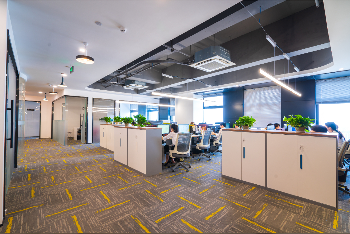
専用の製造および表面実装アセンブリ施設を所有および運営することで、当社はサードパーティの仲介業者を排除します。この垂直統合された製造モデルは、最初の製造可能性設計 (DFM) 検証から最終的なボックスビルド出荷に至るまで、完全なサプライ チェーンの透明性、厳格な品質責任、および工場直接価格設定を保証します。
PCBPath と提携する主な利点
ハードウェア開発スケジュールでは、スピードと妥協のない信頼性の両方が要求されます。当社の製造インフラは、次の 3 つの基本的な柱を中心に設計されています。
- 高度な製造技術: 当社は、複雑な多層、HDI、リジッドフレックス、高周波回路設計をサポートするために、自動レーザー ダイレクト イメージング (LDI)、真空エッチング、UV/CO2 レーザー ドリリング、高速 SMT 配置ラインに継続的に投資しています。
- 超高速の所要時間: 当社の専用のクイックターン試作ラインは 24 時間年中無休で稼働し、ベアボード製造のターンアラウンドを最速で実現します。 24時間 と数日以内の迅速なターンキー PCBA 構築。
- 工場直接のコスト効率: すべてのエンジニアリングレビュー、基板製造、コンポーネント調達、および SMT/THT アセンブリは当社の工場ネットワーク内で直接管理されるため、お客様は隠れたブローカー値上げゼロで業界をリードするコスト構造の恩恵を受けることができます。
エンドツーエンドのターンキー PCB および PCBA ソリューション
ベアボード、電子部品、アセンブリのベンダーを個別に管理すると、通信の遅延や品質リスクが発生します。 PCBPath は、ワークフロー全体を 1 つ屋根の下で管理することで、ハードウェアのライフサイクルを合理化します。
- 制作前 CAM および DFM レビュー: すべてのガーバー、ODB++、および BOM の提出は、次のような包括的なエンジニアリング検査を受けます。 IPC-2221 と IPC-6012 設計ルールは、生産開始前にトレース/スペース、環状リング、インピーダンス、設置面積の問題を解決します。
- 認定コンポーネントの調達: 当社の調達チームは、アクティブおよびパッシブコンポーネントを世界中の認定代理店およびフランチャイズメーカーからのみ調達し、100% のトレーサビリティと偽造リスクゼロを保証します。
- 高精度 PCB 製造: 標準的な 1 ~ 2 層 FR-4 プロトタイプから、32 層高速バックプレーン、メタルコア (MCPCB)、ロジャース RF 基板、ブラインド/埋め込みマイクロビア HDI ボードに至るまで、当社は厳格な寸法公差および電気公差に従って製造しています。
- 自動化された SMT および THT アセンブリ: 当社の組立ラインは、01005 ミニチュア受動部品、ファインピッチ BGA、QFN、POP パッケージ、および完全準拠の選択ウェーブはんだ付けを処理します。 IPC-A-610 クラス 2 およびクラス 3 仕上がり基準。
- 複数段階のテストと品質保証: すべての生産バッチは、フライング プローブまたはフィクスチャの E テスト、3D はんだペースト検査 (SPI)、自動光学検査 (AOI)、BGA ボイドの 3D X 線検査、およびカスタム インサーキット (ICT) または機能テスト (FCT) を受けます。
品質認証と IPC 準拠基準
PCBPath のすべてのプロセスステップには品質が組み込まれています。当社の施設は、厳格な国際的な品質管理システムと環境規制に基づいて運営されています。
| 認証/規格 | 準拠範囲 | お客様のメリット |
|---|---|---|
| ISO 9001:2015 | 販売、エンジニアリング、PCB製造、PCBAアセンブリにわたる品質管理システム | 一貫したバッチ間の再現性と文書化された是正措置のトレーサビリティ |
| UL リスト取得 (E-ファイル認定) | 硬質および多層ラミネートの可燃性および熱安全性準拠 (UL 94V-0) | 商業用、産業用、民生用パワーエレクトロニクスの安全性認証を保証 |
| IPC-A-600 & IPC-6012 | ベアリジッドプリント基板の許容性と性能仕様 (クラス 2 およびクラス 3) | 銅めっきの厚さ、ビアの完全性、絶縁信頼性を検証 |
| IPC-A-610 & J-STD-001 | 電子アセンブリの許容性およびはんだ付けされた電気/電子要件 | 3D AOIとX線検査により検証された高信頼性はんだ接合部 |
| RoHS および REACH への準拠 | 鉛フリーのラミネート、HASL/ENIG 表面仕上げ、および紛争のない材料管理 | 北米、ヨーロッパ、および世界市場参入のための完全な環境コンプライアンス |
当社のグローバルな事業と製造施設
お客様のプロジェクトが、迅速な 5 ピースのエンジニアリング検証プロトタイプ、少量から中量の試験運用、または大量生産を必要とするかどうかにかかわらず、中国全土の当社の専門施設は、世界中の顧客に効率的にサービスを提供できるように戦略的に編成されています。
オペレーション、エンジニアリング、グローバルセールスセンター
にあります 中国上海市青浦区竹営路200号ビル3、当社の国際本社には、CAM/DFM エンジニアリング サポート チーム、コンポーネント調達スペシャリスト、および多言語を話すカスタマー サービス エンジニアがいます。
大量・多層PCB製造工場
にあります 中国江西省吉水県城西工業団地Jingong Avenue、当社の主要なベアボード製造工場には、自動めっきライン、LDI イメージング システム、インピーダンス テスト ラボ、および専用のクイック ターン プロトタイプ ワークショップが備えられています。
高度なターンキー PCB アセンブリ (PCBA) 施設
にあります 中国浙江省平湖市平山大道4965号ビル1の最先端のエレクトロニクス組立工場は、複数の高速 SMT ライン、窒素リフロー オーブン、3D SPI/AOI/X 線検査システム、コンフォーマル コーティング ライン、および機能テスト ステーションを稼働しています。
PCBPath の使命はシンプルです。当社が構築するすべての回路基板の信頼できる品質、透明性の高いエンジニアリング サポート、および迅速な納品によって、世界中のエンジニアと企業を支援することです。
Automated DFM Intelligence
Instant algorithmic design verification scans your Gerber and BOM data to intercept layout risks before fabrication begins.
Uncompromising Quality DNA
Strict IPC Class 2 & Class 3 adherence, multi-stage AOI optical inspection, and complete component traceability.
Turnkey Component Supply Chain
Direct authorized sourcing network with DigiKey, Mouser, and certified tier-1 global distributors ensuring 100% genuine parts.
Industrial Prowess by the Numbers
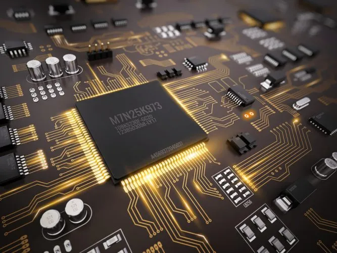
Engineered for extreme reliability, our digital workshops combine high-speed SMT automation with nanometer-calibrated optical verification.
12 Ultra-High-Speed Modular SMT Lines
Powered by Panasonic NPM and Yamaha YRM20 mounters, achieving up to 01005 component placement and 0.3mm fine-pitch BGA mounting with zero misalignment.
160+ Countries Delivery Footprint
Strategic air freight partnerships with DHL, FedEx, and UPS provide expedited customs clearance and direct door-to-door delivery.
Micro-Precision Limits
Capable of fabricating mission-critical aerospace, automotive, and RF medical boards.
Automated Rapid Lane
AI-assisted Gerber DFM review starts the second files upload. High-priority orders jump directly onto dedicated continuous plating lines.
Interactive Smart Workshop Tour
Step inside our automated production lines. Every fabrication milestone is driven by world-class machinery from Japan, Germany, and Switzerland.

Precision Laser Direct Imaging (LDI) Cleanroom
Direct digital imaging transfers CAD artwork directly onto dry film photoresist via high-power solid-state lasers, completely eliminating film dimensional deformation.
Key Technical Parameters
- Resolution / Minimum Trace:2 mil / 2 mil (50 μm)
- Alignment Accuracy:±10 μm (Dynamic Stretch Compensation)
- Cleanroom Standard:Class 10,000 Constant Temp & Humidity
Certified for Mission-Critical Engineering
Audited and certified by leading international testing institutes. Our manufacturing processes strictly comply with automotive, medical, industrial, and consumer electronics criteria.
Quality Management System
Standardized operational quality management across engineering review, raw laminate warehousing, and fabrication.

Automotive Quality Standard
Rigorous automotive PPAP, APQP, and FMEA risk mitigation for high-vibration and extreme-temperature vehicle electronics.
Environmental Management
Green manufacturing protocols with closed-loop wastewater treatment and continuous energy efficiency improvements.

Underwriters Laboratories Safety
Certified flame retardancy and dielectric breakdown safety testing for global export into North American markets.

Hazardous Substance Free
Guaranteed 100% lead-free, cadmium-free, and mercury-free surface finishes including Lead-Free HASL and ENIG.

Chemical Safety Standard
Strict monitoring of Substances of Very High Concern (SVHC) to ensure chemical and human health safety.
IPC Association Member & Calibrated Testing
All fabrication strictly conforms to IPC-A-600 standards for bare boards and IPC-A-610 standards for PCBA soldering. Dedicated cleanrooms and testing labs ensure medical-grade and automotive-grade reliability.
A Trajectory of Relentless Craftsmanship
From rapid bare-board prototyping to an integrated global digital manufacturing network, explore how we evolved.
Establishment of Rapid Prototyping Facility
Founded by senior PCB process engineers in Shenzhen, setting up the first dedicated 24-hour fast-turn rigid PCB prototyping workshop.
Hitachi Laser Drilling & HDI Breakthrough
Commissioned Japanese Hitachi laser micro-drilling systems and German vacuum lamination presses, expanding into 1-3 stage HDI and 32-layer boards.
Automated SMT Assembly & Component Supply Chain
Built our first cleanroom SMT workshop equipped with high-precision Yamaha and Panasonic lines, unlocking one-stop turnkey component procurement and assembly.
Cloud DFM Engine & Digital Smart Factory
Rolled out our proprietary online DFM analysis system and digital MES platform, providing instant quote calculations and automated fabrication tracking.
160+ Countries Network & Green ESG Operations
Established air cargo logistics hubs serving hardware innovators in North America, Europe, and Asia, while obtaining ISO 14001 green factory accreditation.
Ready to Build Your Next Hardware Breakthrough?
Upload your Gerber design and BOM files now. Get instant automated DFM verification, real-time pricing calculations, and expedited global dispatch within seconds.