About PCBPath: Global Fast-Turn PCB Fabrication & Turnkey PCBA Manufacturer
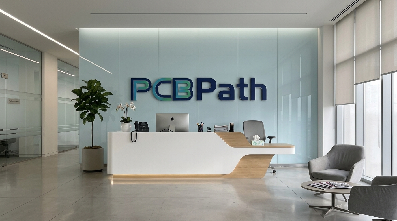
Established in 2015, PCBPath is an ISO-certified direct manufacturer specializing in rapid PCB prototyping, advanced HDI fabrication, and end-to-end turnkey PCBA assembly for global hardware innovators.
Accelerating Electronic Innovation with Intelligent Manufacturing
Established in 2015, PCBPath is an ISO-certified direct manufacturer specializing in rapid PCB prototyping, advanced HDI fabrication, and end-to-end turnkey PCBA assembly for global hardware innovators.
Who We Are: Innovation in Every Layer
Established in 2015, PCBPath is a premier direct manufacturer specializing in high-precision printed circuit board (PCB) fabrication and turnkey PCB assembly (PCBA). We bridge the gap between rapid engineering prototypes and scalable mass production, serving hardware startups, R&D laboratories, and global OEM enterprises across automotive, industrial automation, medical electronics, telecommunications, and IoT sectors.
By owning and operating dedicated fabrication and surface-mount assembly facilities, we eliminate third-party brokers. This vertically integrated manufacturing model guarantees complete supply chain transparency, strict quality accountability, and factory-direct pricing from initial Design for Manufacturability (DFM) verification through final box-build shipment.
Core Advantages of Partnering with PCBPath
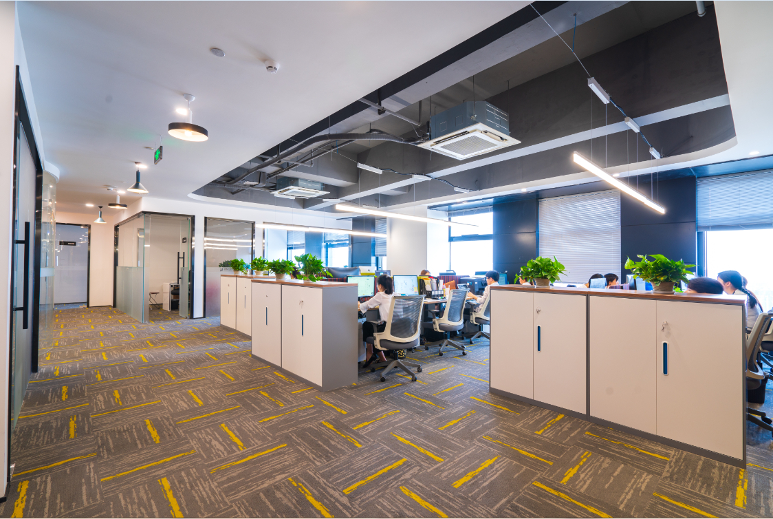
Hardware development schedules demand both speed and uncompromised reliability. Our manufacturing infrastructure is engineered around three foundational pillars:
- Advanced Manufacturing Technology: We continuously invest in automated laser direct imaging (LDI), vacuum etching, UV/CO2 laser drilling, and high-speed SMT placement lines to support complex multilayer, HDI, rigid-flex, and high-frequency circuit designs.
- Ultra-Fast Turnaround Times: Our dedicated quick-turn prototype lines operate 24/7, enabling bare-board fabrication turnarounds as fast as 24 hours and rapid turnkey PCBA builds within days.
- Factory-Direct Cost Efficiency: Because all engineering review, board fabrication, component procurement, and SMT/THT assembly are managed directly within our factory network, customers benefit from industry-leading cost structures with zero hidden broker markups.
End-to-End Turnkey PCB & PCBA Solutions
Managing separate vendors for bare boards, electronic components, and assembly introduces communication delays and quality risks. PCBPath streamlines your hardware lifecycle by managing the entire workflow under one roof:
- Pre-Production CAM & DFM Review: Every Gerber, ODB++, and BOM submission undergoes a comprehensive engineering inspection against IPC-2221 and IPC-6012 design rules to resolve trace/space, annular ring, impedance, and footprint issues before production begins.
- Authorized Component Sourcing: Our procurement team sources active and passive components exclusively from authorized global distributors and franchised manufacturers, ensuring 100% traceability and zero counterfeit risk.
- High-Precision PCB Fabrication: From standard 1–2 layer FR-4 prototypes to 32-layer high-speed backplanes, metal-core (MCPCB), Rogers RF substrates, and blind/buried microvia HDI boards, we manufacture to strict dimensional and electrical tolerances.
- Automated SMT & THT Assembly: Our assembly lines handle 01005 miniature passives, fine-pitch BGAs, QFNs, POP packages, and selective wave soldering in full compliance with IPC-A-610 Class 2 and Class 3 workmanship standards.
- Multi-Stage Testing & Quality Assurance: Every production batch undergoes flying probe or fixture E-test, 3D Solder Paste Inspection (SPI), Automated Optical Inspection (AOI), 3D X-Ray inspection for BGA voiding, and custom In-Circuit (ICT) or Functional Testing (FCT).
Quality Certifications & IPC Compliance Standards
Quality is built into every process step at PCBPath. Our facilities operate under rigorous international quality management systems and environmental regulations:
| Certification / Standard | Scope of Compliance | Customer Benefit |
|---|---|---|
| ISO 9001:2015 | Quality Management System across sales, engineering, PCB fabrication, and PCBA assembly | Consistent batch-to-batch repeatability and documented corrective action traceability |
| UL Listed (E-File Certified) | Flammability and thermal safety compliance (UL 94V-0) for rigid and multilayer laminates | Guaranteed safety certification for commercial, industrial, and consumer power electronics |
| IPC-A-600 & IPC-6012 | Acceptability and performance specifications for bare rigid printed boards (Class 2 & Class 3) | Verified copper plating thickness, via integrity, and dielectric reliability |
| IPC-A-610 & J-STD-001 | Electronic assembly acceptability and soldered electrical/electronic requirements | High-reliability solder joints verified by 3D AOI and X-Ray inspection |
| RoHS & REACH Compliance | Lead-free laminates, HASL/ENIG surface finishes, and conflict-free material management | Full environmental compliance for North American, European, and global market entry |
Our Global Operations & Manufacturing Facilities
Whether your project requires rapid 5-piece engineering validation prototypes, low-to-medium volume pilot runs, or high-volume mass production, our specialized facilities across China are strategically organized to serve global customers efficiently:
Operations, Engineering & Global Sales Center
Located at Building 3, No. 200, Zhuying Road, Qingpu District, Shanghai, China, our international headquarters houses our CAM/DFM engineering support team, component procurement specialists, and multilingual customer service engineers.
High-Volume & Multilayer PCB Manufacturing Plant
Located at Jingong Avenue, Chengxi Industrial Park, Jishui County, Jiangxi Province, China, our primary bare-board fabrication plant features automated plating lines, LDI imaging systems, impedance testing laboratories, and dedicated quick-turn prototype workshops.
Advanced Turnkey PCB Assembly (PCBA) Facility
Located at Building 1, No. 4965, Pingshan Avenue, Pinghu City, Zhejiang Province, China, our state-of-the-art electronics assembly plant operates multiple high-speed SMT lines, nitrogen reflow ovens, 3D SPI/AOI/X-Ray inspection systems, conformal coating lines, and functional test stations.
At PCBPath, our mission is simple: empower engineers and enterprises worldwide with dependable quality, transparent engineering support, and rapid delivery on every circuit board we build.
Automated DFM Intelligence
Instant algorithmic design verification scans your Gerber and BOM data to intercept layout risks before fabrication begins.
Uncompromising Quality DNA
Strict IPC Class 2 & Class 3 adherence, multi-stage AOI optical inspection, and complete component traceability.
Turnkey Component Supply Chain
Direct authorized sourcing network with DigiKey, Mouser, and certified tier-1 global distributors ensuring 100% genuine parts.
Industrial Prowess by the Numbers
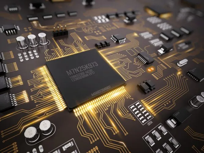
Engineered for extreme reliability, our digital workshops combine high-speed SMT automation with nanometer-calibrated optical verification.
12 Ultra-High-Speed Modular SMT Lines
Powered by Panasonic NPM and Yamaha YRM20 mounters, achieving up to 01005 component placement and 0.3mm fine-pitch BGA mounting with zero misalignment.
160+ Countries Delivery Footprint
Strategic air freight partnerships with DHL, FedEx, and UPS provide expedited customs clearance and direct door-to-door delivery.
Micro-Precision Limits
Capable of fabricating mission-critical aerospace, automotive, and RF medical boards.
Automated Rapid Lane
AI-assisted Gerber DFM review starts the second files upload. High-priority orders jump directly onto dedicated continuous plating lines.
Interactive Smart Workshop Tour
Step inside our automated production lines. Every fabrication milestone is driven by world-class machinery from Japan, Germany, and Switzerland.

Precision Laser Direct Imaging (LDI) Cleanroom
Direct digital imaging transfers CAD artwork directly onto dry film photoresist via high-power solid-state lasers, completely eliminating film dimensional deformation.
Key Technical Parameters
- Resolution / Minimum Trace:2 mil / 2 mil (50 μm)
- Alignment Accuracy:±10 μm (Dynamic Stretch Compensation)
- Cleanroom Standard:Class 10,000 Constant Temp & Humidity
Certified for Mission-Critical Engineering
Audited and certified by leading international testing institutes. Our manufacturing processes strictly comply with automotive, medical, industrial, and consumer electronics criteria.
Quality Management System
Standardized operational quality management across engineering review, raw laminate warehousing, and fabrication.

Automotive Quality Standard
Rigorous automotive PPAP, APQP, and FMEA risk mitigation for high-vibration and extreme-temperature vehicle electronics.
Environmental Management
Green manufacturing protocols with closed-loop wastewater treatment and continuous energy efficiency improvements.

Underwriters Laboratories Safety
Certified flame retardancy and dielectric breakdown safety testing for global export into North American markets.

Hazardous Substance Free
Guaranteed 100% lead-free, cadmium-free, and mercury-free surface finishes including Lead-Free HASL and ENIG.

Chemical Safety Standard
Strict monitoring of Substances of Very High Concern (SVHC) to ensure chemical and human health safety.
IPC Association Member & Calibrated Testing
All fabrication strictly conforms to IPC-A-600 standards for bare boards and IPC-A-610 standards for PCBA soldering. Dedicated cleanrooms and testing labs ensure medical-grade and automotive-grade reliability.
A Trajectory of Relentless Craftsmanship
From rapid bare-board prototyping to an integrated global digital manufacturing network, explore how we evolved.
Establishment of Rapid Prototyping Facility
Founded by senior PCB process engineers in Shenzhen, setting up the first dedicated 24-hour fast-turn rigid PCB prototyping workshop.
Hitachi Laser Drilling & HDI Breakthrough
Commissioned Japanese Hitachi laser micro-drilling systems and German vacuum lamination presses, expanding into 1-3 stage HDI and 32-layer boards.
Automated SMT Assembly & Component Supply Chain
Built our first cleanroom SMT workshop equipped with high-precision Yamaha and Panasonic lines, unlocking one-stop turnkey component procurement and assembly.
Cloud DFM Engine & Digital Smart Factory
Rolled out our proprietary online DFM analysis system and digital MES platform, providing instant quote calculations and automated fabrication tracking.
160+ Countries Network & Green ESG Operations
Established air cargo logistics hubs serving hardware innovators in North America, Europe, and Asia, while obtaining ISO 14001 green factory accreditation.
Ready to Build Your Next Hardware Breakthrough?
Upload your Gerber design and BOM files now. Get instant automated DFM verification, real-time pricing calculations, and expedited global dispatch within seconds.